HMC565-Die - Low Noise Amplifier Chip, 6 - 20 GHz
HMC565-Die是AD公司的一款低噪声放大器产品,HMC565-Die是Low Noise Amplifier Chip, 6 - 20 GHz,本站介绍了HMC565-Die的封装应用图解、特点和优点、功能等,并给出了与HMC565-Die相关的AD元器件型号供参考。
HMC565-Die - Low Noise Amplifier Chip, 6 - 20 GHz - 低噪声放大器 - 放大器 - Analog Devices, LLC
产品描述
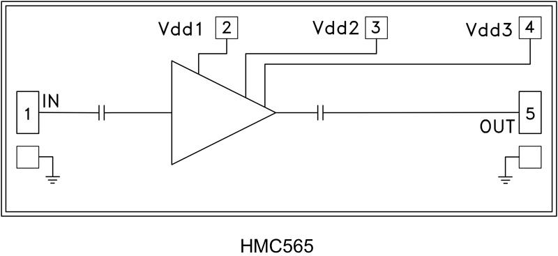
The HMC565 is a high dynamic range GaAs PHEMT MMIC Low Noise Amplifier (LNA) chip which operates from 6 to 20 GHz. The HMC565 features 22 dB of small signal gain, 2.3 dB of noise figure and has a consistent IP3 of 20 dBm across the operating band. This self-biased LNA is ideal for hybrid and MCM assemblies due to its compact size, wideband performance, single +3V supply operation, and DC blocked RF I/O’s. All data is measured with the chip in a 50 Ohm test fixture connected via two 0.025 mm (1 mil) diameter bondwires of minimal length 0.31 mm (12 mil).
Applications
Point-to-Point Radios Point-to-Multi-Point Radios & VSAT Test Equipment and Sensors Military & Space优势和特点
Noise Figure: 2.3 dBGain: 22 dBOIP3: 20 dBmSingle Supply: +3V @ 53mA50 Ohm Matched Input/OutputSmall size: 2.53 x 0.98 x 0.10 mm
下面可能是您感兴趣的AD公司低噪声放大器元器件
AD8505 - 单路、20 μA(最大值)、轨到轨I/O、零输入交越失真放大器HMC439 - 数字鉴相鉴频器,采用SMT封装,0.01 - 1.3 GHzADIS16405 - High Precision Tri-Axis Gyroscope, Accelerometer, MagnetometerADM812 - Microprocessors Supervisory Circuit in 4-Lead SOT-143, Logic High RESET OutputAD7924 - 内置序列器的4通道、1 MSPS、12位模数转换器,采用16引脚TSSOP封装ADN2913 - Continuous Rate 6.5 Mbps to 8.5 Gbps Clock and Data Recovery IC with Integrated Limiting Amp/EQHMC646 - 40W SPDT Failsafe Switch SMT, 0.1 - 2.1 GHzAD5343 - +2.5V至5.5V、230 μA、双通道、轨到轨电压输出12位DAC,内置字节载入并行接口,采用20引脚TSSOP封装ADA4622-2 - 30V、7.5 MHz、低偏置电流、单电源、RRO、精密运算放大器AD8418 - 双向、零漂移电流检测放大器